1. Fabrication of Nanowires at Surfaces
The goal of this project is the design of artificial materials that consist of ultrafine wires or linear arrays of dots, ten to hundred times finer than those produced with commercial micro-structure fabrication techniques. In fact, it has become possible to shrink nanowires all the way down to their ultimate limit, that is, metallic atom chains on a non-metallic substrate. These form spontaneously on many stepped semiconductor surfaces (see Sections 2 and 3 below and an overview talk on atomic and molecular wires).
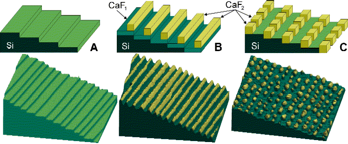
An important aspect in fabricating nanowires is the ability to prepare wires on many materials with adjustable thickness. In particular, using silicon wafers as substrate is highly desirable. To achieve this goal we suggest the following "universal" process. First, a silicon substrate with a regular array of steps is prepared (A). Then, stripes (B) or dots (C) of a passivating material are attached to the step edges. This part is analogous to creating a photoresist mask in traditional lithography. As mask material we use calcium fluoride, which is lattice-matched to silicon and chemically inert. Eventually, the desired material is deposited on the remaining silicon, for example by substrate-selective chemical vapor deposition (CVD) or electroplating. Alternatively, calcium fluoride could become useful as an etch mask for producing trenches in the silicon that can be filled with new materials to achieve a planar structure.
The figure below shows the preparation of calcium fluoride masks in schematic form (top), together with actual data (bottom).
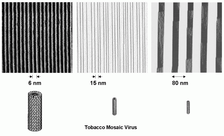
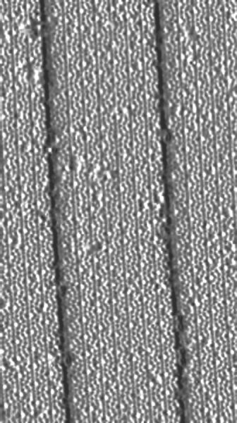
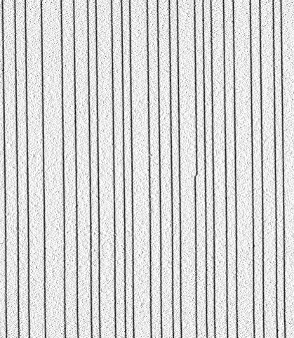
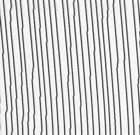
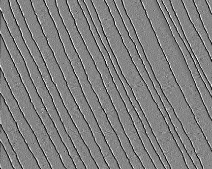
To start along this pathway, we determine the conditions for obtaining highly-regular step structures on silicon. The images below demonstrate the range of step arrays that can be formed on silicon surfaces by self-assembly. Typically, the step spacing is comparable to the size of a virus. These images are taken with a scanning tunneling microscope (STM). They show the derivative of the tip height. That gives the impression of a surface illuminated from the left, with the steps casting dark shadows to the right.
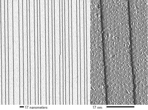
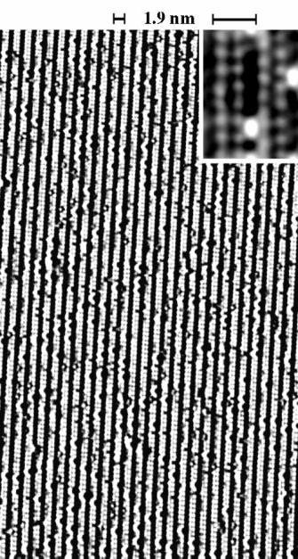
Particularly perfect step arrays
could be achieved on the Si(111)7x7 surface. The 7x7 structure causes
steps running along the [011]-direction to become extremely straight,
because each kink requires generating 14 new rows of silicon atoms (7 rows,
two layers deep). The step edges are atomically-straight with a kink spacing
as low as a single kink in 20,000 atoms, as seen in the image
below. These are taken with a scanning tunneling microscope (STM). The
x-derivative of the topography is displayed, which makes steps appear as
dark lines. The image on the right zooms in on the terrace between two
steps (heavy dark lines). The atomic pattern of the 7x7 structure structure
is resolved, which has fine grooves built in that run parallel to the step edges.
These grooves are 2.3 nm apart and determine the location of possible
step edges. They may be viewed as the LEGO blocks of the
aspiring nano-engineer.
Fabrication of straight steps: J. Viernow et al., Appl. Phys. Lett. 72, 948 (1998);
Single steps and bunched steps: J.-L. Lin et al., J. Appl. Phys. 84, 255 (1998).
Atomically-perfect steps: A. Kirakosian et al., Appl. Phys. Lett. 79, 1608 (2001).
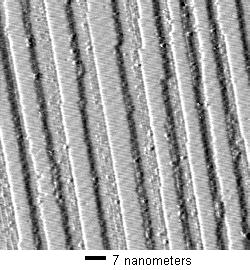
Our "universal process" can be carried further by
producing a calcium fluoride mask, as shown in the image below.
A stepped silicon surface is coated with a layer of CaF1
and CaF2 stripes are formed on top of that layer.
These stripes are are continuous and do not touch each other,
because adjacent stripes cannot bond to each other.
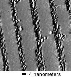
The stripe width of 7 nm achieved here is well below
the resolution of 180 nm achieved in commercial lithography
for chip fabrication.
J. Viernow et al., Appl. Phys. Lett. 74, 2125 (1999).
The third step of the "universal
process" involves selective deposition or etching
between the masked areas. The picture below shows that
molecules can be deposited selectiveley in the CaF1
grooves between CaF2 stripes.
H. Rauscher, et al., Chem. Phys. Lett. 303, 363 (1999).
Using organometallic molecules, such as ferrocene, it is possible
to fabricate iron wires 3 nanometers wide.
J.-L. Lin et al., Appl. Phys. Lett. 78, 829 (2001).
Images (derivative of the topography, "illuminated from the side")
Si(111)7x7 closeup, showing the corner holes and grooves of the 7x7 cell.
Step array on silicon with only a single kink in 20,000 edge atoms.
Steps and kinks on silicon
Large array of CaF2 stripes
3 nm copper wires on molybdenum, made visible by image state contrast.
2. Atom Chains, the Ultimate Nanowires
The complete set of quantum numbers for electrons in a solid is revealed by angle-resolved photoemission with tunable synchrotron radiation. The two principal quantum numbers energy and momentum are combined in a band structure plot, as in the picture below. The dark bands represent regions with high photoemission intensity. With multitedection techniques for energy and angle it is now possible to see the band structure directly on a television screen.
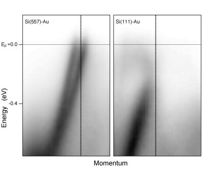
Some of the atomic wires are found to be metallic (above left). The metallic behavior is deduced from the observation that the bands extend all the way up to the Fermi level EF for Si(557)-Au, as in a metal. By way of contrast, the flat Si(111)-Au surface in the panel on the right shows a band that does not reach EF. Even though the metal atoms are strongly coupled to the substrate, metallic electrons do not interact with the silicon substrate because their energy lies in the band gap of silicon.
Electrons at the Fermi level are particularly interesting because they assemble themselves into exotic phases in low dimensions. These electrons are best characterized by the Fermi surface, which describes their momentum distribution. Such Fermi surfaces are shown below for two- and one-dimensional electrons at silicon surfaces with extra metal atoms (typically a monolayer for a 2D structure and 1/5 of a monolayer for a 1D structure). Two-dimensional Fermi surfaces typically consist of circles (top), which may form intricate patterns by replication at a superlattice (middle). One-dimensional Fermi surfaces are straight lines, which become modulated by small wiggles if a weak two-dimensional coupling is present between the atom chains (bottom).
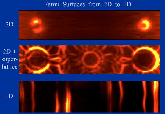
Currently, we are exploring silicon surfaces with a variety of step spacings. That makes it possible to vary the dimensionality between 2D and 1D. For example, the coupling ratio parallel/perpendicular to the chains can be varied from 10:1 to >70:1. In addition, structures with fractional filling can be produced, such as for the one-dimensional Fermi surface shown above. Fractional filling is achieved by embedding the chains into a 2D superlattice where silicon atoms act as dopants, as in modulation doping of semiconductors. That raises interesting questions about an analog to the fractional quantum Hall effect in a one-dimensional electron gas. Chains can be formed not only with gold atoms, but also with a large variety of other metal atoms. These include magnetic atoms, such as Gd and other rare earths, which open up possibilities of fabricating spin chains. In fact, even non-magnetic gold chains form spin-split Fermi surfaces, as in the example above. That is due to the spin-orbit interaction in the reduced symmetry of a surface. Another chain structure spontaneously decomposes into metallic and semiconducting segments, which can be viewed as the one-dimensional analog of stripes, which have been a hot topic in the context of high temperature superconductivity. All these atomic chain structures form an ideal playground to search for interesting new phases of matter in one dimension.
2D Fermi surfaces: J.N. Crain et al., Phys. Rev. B 66, 205302 (2002).
1D Fermi surfaces: J.N. Crain et al., Phys. Rev. Lett. 90, 176805 (2003).
Gd chains: A. Kirakosian et al., Surf. Sci. 498, L109 (2002).
Spin splitting: I. Barke et al., Phys. Rev. Lett. 97, 226405 (2006).
Review: I. Barke et al., Solid State Commun. 142, 617 (2007).
3. Spin Chains for Single Spin Electronics
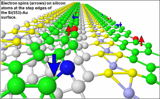
Steven C. Erwin and F. J. Himpsel, Intrinsic magnetism at silicon surfaces, Nature Communications 1:58 (2010).
P. C. Snijders et al., Spectroscopic evidence for spin-polarized edge states in graphitic Si nanowires,
New Journal of Physics 14, 103004 (2012).
K. Biedermann et al., Spin-split silicon states at step edges of Si(553)-Au,
Phys. Rev. B 85, 245413 (2012).
S. Polei et al., Structural Transition in Atomic Chains Driven by Transient Doping, Phys. Rev. Lett. 111, 156801 (2013).
Overview talk on Atomic and Molecular Wires